

Description
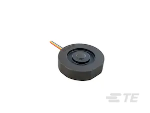
FC29 Compression Load Cell
TE Connectivity’s (TE) FX29 is a compact compression load cellthat offers exceptional price-to-performance in a robust sensorpackage. Optimized for embedded force sensing applications fromdisposable medical devices to durable appliances and exerciseequipment. The FX29 allows design flexibility with mV, amplified,and digital output options.The FX29 incorporates the high reliability Microfused technologyand is offered in ranges from 10lbf to 200lbf (50N to 1000N).Microfused technology provides excellent span and zero stability,outstanding cycle life, superior resolution, high over-rangecapabilities, and an unamplified span sensitivity of 20mV/V.The FX29 utilizes a two-piece construction of stainless steelmaterials. The combination of a metal injection molded flexure andmicro miniaturized MEMS strain gauges allows flexibility of forcerange options for a lower cost sensor. These improvements overprevious load cell designs give the FX29 more precisedimensional control and better performance.
Features
• Compact Design
• mV or Amplified Analog Outputs
• Optional I2C Digital Interface
• High Over Range Capability
Applications
• Medical Infusion Pumps
• Analog & Digital Scales
• Fitness & Exercise Equipment
• Payload Weighing
• Power Tools
• Robotics
• Surgical & Dental Tools
• Battery Powered Devices
• Manufacturing Equipment
STANDARD RANGES
Absolute Maximum Ratings (Analog) (1)
| Parameter | Symbol | Min | Typ | Max | Units | Notes / Conditions |
|---|---|---|---|---|---|---|
| Supply Voltage (Analog mV Output) | Vdd | 6.0 | V | Analog mV Output | ||
| Supply Voltage (Analog 0.5–4.5V Output) | Vdd | 5.25 | V | Analog 0.5–4.5V Output | ||
| Storage Temperature | TS | -40 | +85 | °C | ||
| Compressive Load | Lmax | 2.5× Rated | ||||
| ESD (Human Body Model) | -4.0 | 4.0 | kV | Human Body Model |
(1) Maximum limits the device will withstand without damage
| Pounds-Force (lbf) | Newtons (N) |
|---|---|
| 10 | 50 |
| 25 | 125 |
| 50 | 250 |
| 100 | 500 |
| 200 | 1000 |
Electrical Specifications (Analog)
(Unless otherwise specified, all parameters are measured at 25°C @ 5.0V applied)
| Parameter | Symbol | Min | Typ | Max | Units | Notes / Conditions |
|---|---|---|---|---|---|---|
| Supply voltage (mV Output only) | Vdd | 1.00 | — | 6.0 | V | mV Output only |
| Supply voltage (0.5–4.5V Output only) | Vdd | 4.75 | — | 5.25 | V | 0.5–4.5V Output only |
| Operating current | Idd | — | 3 | — | mA | 0.5–4.5V Output only |
| Input resistance | Rin | 2.4 | 3.0 | 3.6 | kΩ | mV Output only |
| Output resistance | Rout | 1.76 | 2.2 | 2.64 | kΩ | mV Output only |
| Rise time | Tr | — | 2.0 | — | ms | 10% to 90% |
| Maximum output current | Io | — | — | 2.2 | mA | 0.5–4.5V Output only |
| Output short circuit duration | Ts | — | — | ∞ | seconds | 0.5–4.5V Output only |
| Insulation resistance | — | 50 | — | — | MΩ | @ 250 VDC |
| Sampling rate | — | — | 1.0 | — | kHz | — |
Operating Specifications (Analog)
(Unless otherwise specified, all parameters are measured at 25°C @ 5.0V applied)
| Parameter | Symbol | Min | Typ | Max | Units | Notes / Conditions |
|---|---|---|---|---|---|---|
| Zero offset¹ (mV Output only) | — | -15 | — | 15 | mV/V | mV Output only |
| Zero offset¹ (0.5–4.5V Output only) | — | 300 | 500 | 700 | mV | 0.5–4.5V Output only |
| Full scale span¹ (mV Output only) | — | 16 | 20 | 24 | mV/V | mV Output only |
| Full scale span¹ (0.5–4.5V Output only) | — | 3800 | 4000 | 4200 | mV | 0.5–4.5V Output only |
| Non-linearity | — | -1 | — | 1 | %Span | BFSL |
| Hysteresis | — | -0.8 | — | 0.8 | %Span | — |
| Zero repeatability | — | -0.8 | — | 0.8 | %Span | — |
| Span repeatability | — | -0.8 | — | 0.8 | %Span | — |
| Thermal shift for zero | — | -0.05 | — | 0.05 | %Span/°C | Reference to 25°C |
| Thermal shift for span | — | -0.05 | — | 0.05 | %Span/°C | Compensated temperature range |
| Cycle life | — | 1E+6 | — | — | cycles | 0 to full scale |
| Deflection at rated load | — | — | 0.03 | — | mm | — |
| Weight | — | — | 6.0 | — | grams | Without ribbon cable |
(1) Span and zero offset are ratiometric to power supply voltage
Environmental Specifications (Analog)
(Unless otherwise specified, all parameters are measured at 25°C @ 5.0V applied)
| Parameter | Symbol | Min | Typ | Max | Units | Notes / Conditions |
|---|---|---|---|---|---|---|
| Compensated temperature range | To | 0 | — | 50 | °C | 0.5–4.5V Output only |
| Storage temperature | Ts | -40 | — | 85 | °C | — |
| Ambient humidity | — | 0 | — | 85 | %RH | Non-condensing |
| EMI / RFI / ESD protection | — | — | — | — | — | IEC61000-4-2 (8 kV air / 4 kV contact); IEC61000-4-3 (3 V/m); EN55032 Class A; mV Output only |
| Ingress protection | — | — | — | IP43 | — | — |
| Media compatibility | — | — | — | — | — | External exposed surfaces: 17-4 and 304 stainless steel (excluding cable & connector) |
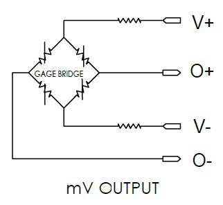
Schematic Diagram – mV output (Analog)
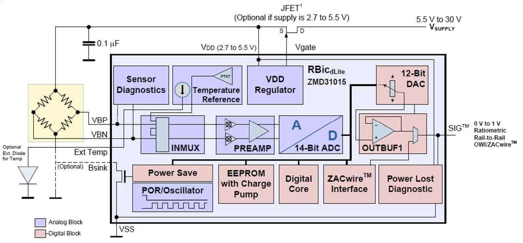
Block Diagram – 0.5 to 4.5V output (Analog)
Absolute Maximum Ratings (Digital) (1)
| Parameter | Symbol | Min | Typ | Max | Units | Notes / Conditions |
|---|---|---|---|---|---|---|
| Supply voltage | — | — | — | 5.50 | V | — |
| Storage temperature | Ts | -40 | — | +85 | °C | — |
| Compressive load | Lmax | — | — | 2.5 × Rated | — | — |
| ESD (Human Body Model) | — | -4.0 | — | 4.0 | kV | Human Body Model |
(1) Maximum limits the device will withstand without damage
Standard Load Ranges
| Pounds-Force (lbf) | Newtons (N) |
|---|---|
| 10 | 50 |
| 25 | 125 |
| 50 | 250 |
| 100 | 500 |
| 200 | 1000 |
Electrical Specifications (Digital)
(Unless otherwise specified, all parameters are measured at 25°C @ 3.0V applied)
| Parameter | Symbol | Min | Typ | Max | Units | Notes / Conditions |
|---|---|---|---|---|---|---|
| Supply voltage (Vsupply) | Vdd | 2.7 | — | 5.5 | V | — |
| Operating current | Idd | — | 3 | — | mA | — |
| Sleep mode current | Islp | 0.5 | — | 5 | μA | — |
| Insulation resistance | — | 50 | — | — | MΩ | @ 250 VDC |
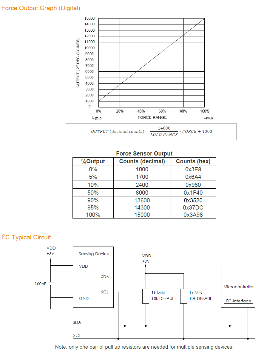
Force Operating Specifications (Digital)
(Unless otherwise specified, all parameters are measured at 25°C @ 3.0V applied)
| Parameter | Symbol | Min | Typ | Max | Units | Notes / Conditions |
|---|---|---|---|---|---|---|
| Zero offset | — | 300 | 1000 | 1700 | Counts (Base10) | — |
| Full scale span | — | 14300 | 15000 | 15700 | Counts (Base10) | — |
| Non-linearity | — | -1 | — | 1 | %Span | BFSL |
| Hysteresis | — | -0.8 | — | 0.8 | %Span | — |
| Zero repeatability | — | -0.8 | — | 0.8 | %Span | — |
| Span repeatability | — | -0.8 | — | 0.8 | %Span | — |
| Thermal shift for zero | — | -0.05 | — | 0.05 | %Span/°C | Reference to 25°C |
| Thermal shift for span | — | -0.05 | — | 0.05 | %Span/°C | Compensated temperature range |
| Cycle life | — | 1E+6 | — | — | cycles | 0 to full scale |
| A/D resolution | — | — | 14 | — | Bits | — |
| Response time (non-sleep mode) | — | — | 3 | — | ms | 4 MHz, non-sleep mode |
| Response time (sleep mode) | — | — | 8.4 | — | ms | 4 MHz, sleep mode |
| Deflection at rated load | — | — | 0.03 | — | mm | — |
| Weight | — | — | 6.0 | — | grams | Without ribbon cable |
Environmental Specifications (Digital)
(Unless otherwise specified, all parameters are measured at 25°C @ 3.0V applied)
| Parameter | Symbol | Min | Typ | Max | Units | Notes / Conditions |
|---|---|---|---|---|---|---|
| Compensated temperature range | To | 0 | — | 50 | °C | — |
| Storage temperature | Ts | -40 | — | 85 | °C | — |
| Ambient humidity | — | 0 | — | 85 | %RH | Non-condensing |
| Ingress protection | — | — | — | IP43 | — | — |
| Media compatibility | — | — | — | — | — | External exposed surfaces: 17-4 and 304 stainless steel (excluding cable & connector) |
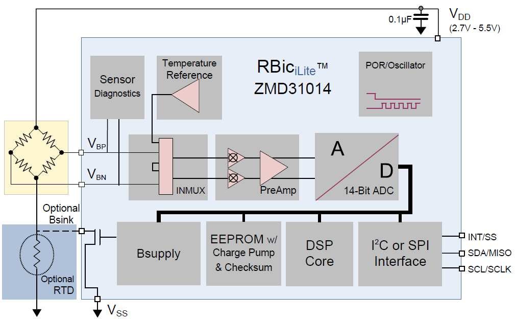
Block Diagram – I2C Digital Output (Digital)
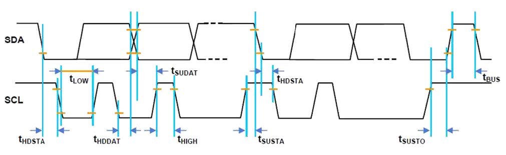
I2C Interface
| Parameter | Symbol | Min | Typ | Max | Units | Notes / Conditions |
|---|---|---|---|---|---|---|
| SCLK clock frequency | FSCL | 100 | — | 400 | kHz | — |
| Start condition hold time relative to SCL edge | tHOSTA | 0.1 | — | — | μs | — |
| Minimum SCL clock low width¹ | tLOW | 0.6 | — | — | μs | — |
| Minimum SCL clock high width¹ | tHIGH | 0.6 | — | — | μs | — |
| Start condition setup time relative to SCL edge | tSUSTA | 0.1 | — | — | μs | — |
| Data hold time on SDA relative to SCL edge | tHDDAT | 0 | — | — | μs | — |
| Data setup time on SDA relative to SCL edge | tSUDAT | 0.1 | — | — | μs | — |
| Stop condition setup time on SCL | tSUSTO | 0.1 | — | — | μs | — |
| Bus free time between stop and start condition | tBUS | 2 | — | — | μs | — |
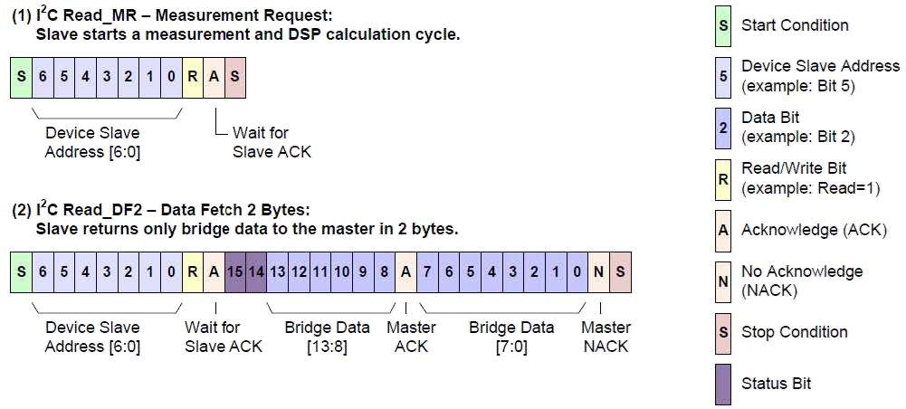
I2C Interface Timing Diagram
Digital Input and Output Parameters
(Unless otherwise specified, all parameters are measured at 25°C @ 3.0V applied)
| Parameter | Symbol | Min | Typ | Max | Units | Notes / Conditions |
|---|---|---|---|---|---|---|
| Input high voltage | VIH | 0.8 × Vdd | — | 1.0 × Vdd | — | — |
| Input low voltage | VIL | 0.0 | — | 0.2 × Vdd | V | — |
| Output low level | — | — | — | — | — | x Vdd |
| Load capacitance @ SDA | — | — | — | 200 | pF | @ 400 kHz |
| Input capacitance (each pin) | — | — | 10 | — | pF | — |
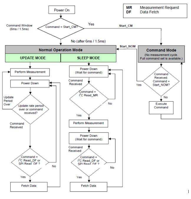
I2C Measurement Packet Read Sequence
General Working Mode
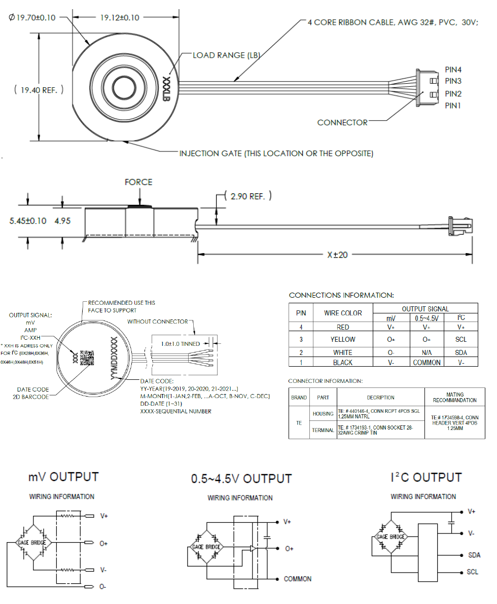
Outline Drawing and Connections
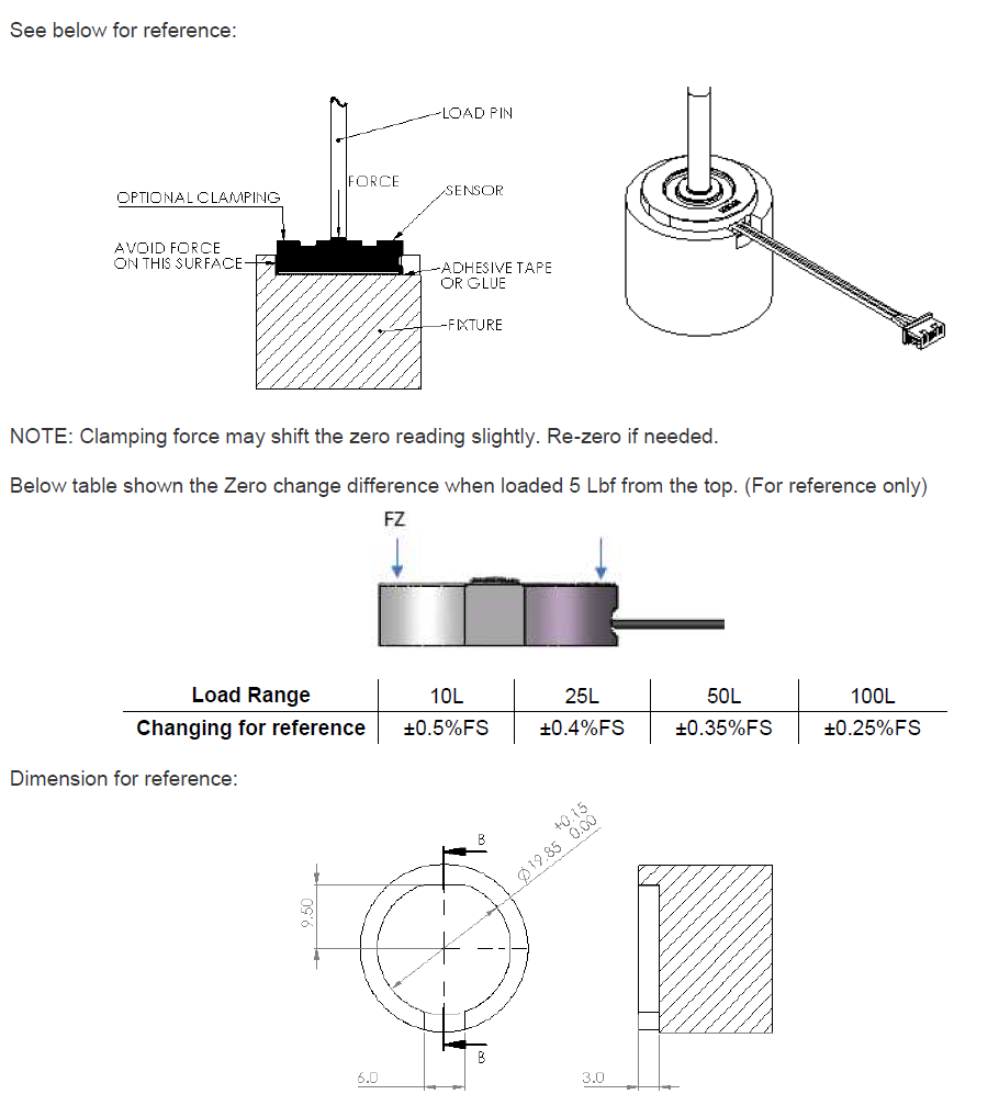
Mounting Recommendation
The sensor can be put into a simple slot fixture for load testing. The load should be applied to the spherical face
of center boss. Recommended to stick the sensor with double face 3M adhesive or glue. Some feature to clamp
the sensor from top to down can be optional.
ORDERING INFORMATION
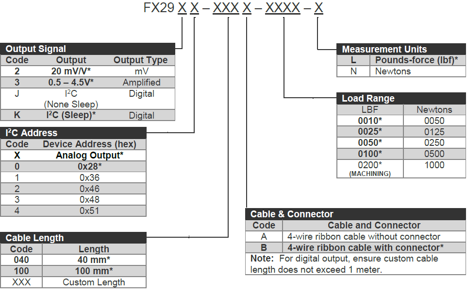
*Sensor features shown in bold are typically stocked by our distribution partners, or available with short lead times from the
factory depending on availability. For customizing cable length, require 500 pcs of MOQ. Contact customer service for details.
Reviews
There are no reviews yet.